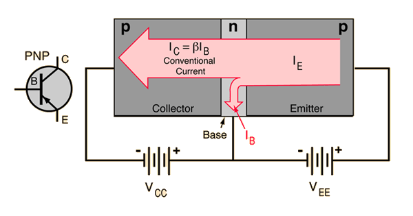
Transistor as Current Amplifier
The larger collector current IC is proportional to the base current IB according to the relationship IC =βIB , or more precisely it is proportional to the base-emitter voltage VBE . The smaller base current controls the larger collector current, achieving current amplification.
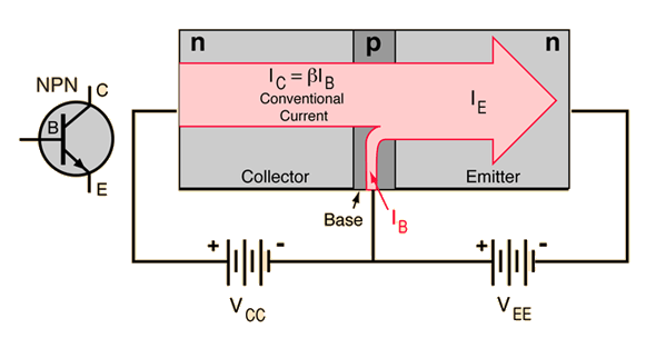
The analogy to a valve is sometimes helpful. The smaller current in the base acts as a "valve", controlling the larger current from collector to emitter. A "signal" in the form of a variation in the base current is reproduced as a larger variation in the collector-to-emitter current, achieving an amplification of that signal.
|