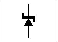
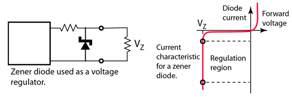
The Zener Effect

With the application of sufficient reverse voltage, a p-n junction will experience a rapid avalanche breakdown and conduct current in the reverse direction. Valence electrons which break free under the influence of the applied electric field can be accelerated enough that they can knock loose other electrons and the subsequent collisions quickly become an avalanche. When this process is taking place, very small changes in voltage can cause very large changes in current. The breakdown process depends upon the applied electric field, so by changing the thickness of the layer to which the voltage is applied, zener diodes can be formed which break down at voltages from about 4 volts to several hundred volts.
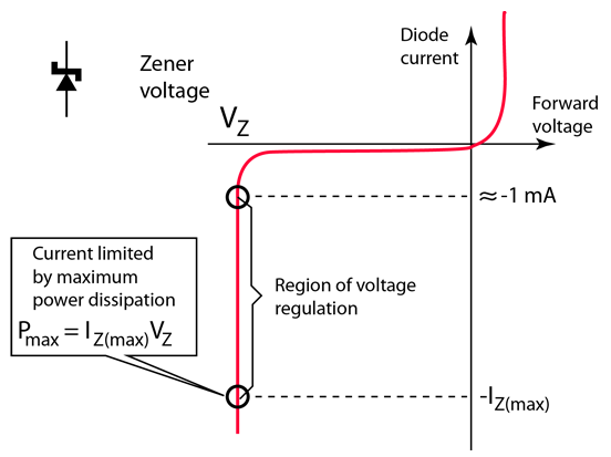
Zener applications Zener diode zener regulator
Index

Semiconductor concepts

Semiconductors for electronics

Electronics concepts
 
HyperPhysics***** Condensed Matter R Nave
Go Back


Zener Diode

The zener diode uses a p-n junction in reverse bias to make use of the zener effect, which is a breakdown phenomenon which holds the voltage close to a constant value called the zener voltage. It is useful in zener regulators to provide a more constant voltage, for improvement of regulated power supplies, and for limiter applications.
Zener effectZener current characteristics Zener applications
Index

Semiconductor concepts

Semiconductors for electronics

Electronics concepts
 
HyperPhysics***** Condensed Matter R Nave
Go Back


Tunnel Diode Characteristic

In 1957, Esaki, Kurose and Suzuki discovered that quantum mechanical tunneling of electrons could be achieved in a solid state diode. Josephson had discovered tunneling characteristics in the Josephson junction for superconductors. Esaki and Josephson shared the 1973 Nobel Prize for these discoveries.
In the case of the tunnel diode, the conditions for tunneling were achieved by more heavily doping the semiconductors associated with the pn junction. With germanium or gallium arsenide the depletion layer at the junction was very narrow, and permitted electrons to tunnel across the barrier. For very low reverse voltages through small positive voltages, the tunneling increased and the junction acted like a conductor.

For small forward bias, electrons tunnel across the depletion region from the P to the N side and fill states in the conduction band on the N-side. They align with hole states on the P-side. With increasing forward voltage, there is increasing misalignment and the current begins to drop with increasing forward voltage, producing a "negative resistance" behavior. For higher forward voltages, the junction begins to act like a normally forward biased diode, but the negative resistance regime was found to be very useful in producing oscillators.

Tunnel diode oscillators were found to be very useful through the 1970s as high-frequency oscillators and found use in the space program. They have since been mostly replaced with a variety of other oscillator types.

Circuit symbolApplication in oscillator
Index

Semiconductor concepts

Semiconductors for electronics

Electronics concepts

Tunnel diode, Wiki

Floyd, Electronic Devices,
Ch 3-5
 
HyperPhysics***** Condensed Matter R Nave
Go Back