P-N Energy Bands

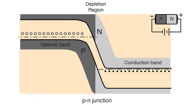
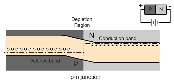
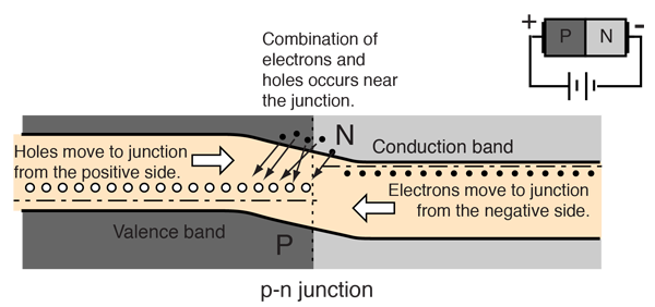
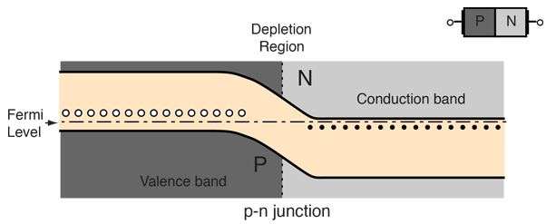
For a p-n junction at equilibrium, the fermi levels match on the two sides of the junctions. Electrons and holes reach an equilibrium at the junction and form a depletion region. The upward direction in the diagram represents increasing electron energy. That implies that you would have to supply energy to get an electron to go up on the diagram, and supply energy to get a hole to go down.

Index

Semiconductor concepts

Semiconductors for electronics
 
HyperPhysics***** Condensed Matter R Nave
Go Back


P-N Energy Bands

To reverse-bias the p-n junction, the p side is made more negative, making it "uphill" for electrons moving across the junction. The conduction direction for electrons in the diagram is right to left, and the upward direction represents increasing electron energy.

Index

Semiconductor concepts

Semiconductors for electronics
 
HyperPhysics***** Condensed Matter R Nave
Go Back


P-N Energy Bands

To forward bias the p-n junction, the p side is made more positive, so that it is "downhill" for electron motion across the junction. An electron can move across the junction and fill a vacancy or "hole" near the junction. It can then move from vacancy to vacancy leftward toward the positive terminal, which could be described as the hole moving right. The conduction direction for electrons in the diagram is right to left, and the upward direction represents increasing electron energy.

Show more detail on conduction under forward bias.
Index

Semiconductor concepts

Semiconductors for electronics
 
HyperPhysics***** Condensed Matter R Nave
Go Back


Forward Biased Conduction

When the p-n junction is forward biased, the electrons in the n-type material which have been elevated to the conduction band and which have diffused across the junction find themselves at a higher energy than the holes in the p-type material. They readily combine with those holes, making possible a continuous forward current through the junction.

Show more detail about charge carriers.
Index

Semiconductor concepts

Semiconductors for electronics
 
HyperPhysics***** Condensed Matter R Nave
Go Back


Forward Biased Conduction

The forward current in a p-n junction when it is forward-biased (illustrated below) involves electrons from the n-type material moving leftward across the junction and combining with holes in the p-type material. Electrons can then proceed further leftward by jumping from hole to hole, so the holes can be said to be moving to the right in this process.

Index

Semiconductor concepts

Semiconductors for electronics
 
HyperPhysics***** Condensed Matter R Nave
Go Back