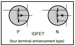
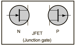
Junction Field Effect Transistor

The common transistor is called a junction transistor, and it was the key device which led to the solid state electronics revolution. In application, the junction transistor has the disadvantage of a low input impedance because the base of the transistor is the signal input and the base-emitter diode is forward biased. Another device achieved transistor action with the input diode junction reversed biased, and this device is called a "field effect transistor" or a "junction field effect transistor", JFET. With the reverse biased input junction, it has a very high input impedance. Having a high input impedance minimizes the interference with or "loading" of the signal source when a measurement is made.

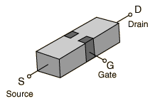
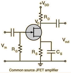
For an n-channel FET, the device is constructed from a bar of n-type material, with the shaded areas composed of a p-type material as a Gate. Between the Source and the Drain, the n-type material acts as a resistor. The current flow consists of the majority carriers (electrons for n-type material).

Characteristic curves
Common source amplifier

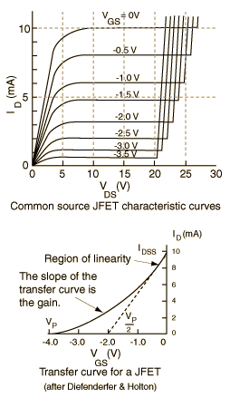
Since the Gate junction is reverse biased and because there is no minority carrier contribution to the flow through the device, the input impedance is extremely high.

The control element for the JFET comes from depletion of charge carriers from the n-channel. When the Gate is made more negative, it depletes the majority carriers from a larger depletion zone around the gate. This reduces the current flow for a given value of Source-to-Drain voltage. Modulating the Gate voltage modulates the current flow through the device.

Index

Electronics concepts

Transistor varieties

Reference
Diefenderfer & Holton
Sec 8-7
 
HyperPhysics*****Electricity and magnetismR Nave
Go Back


IGFET

The insulated gate field effect transistor (IGFET) differs from the JFET by the addition of a silicon dioxide layer over the JFET and then a layer of silicon nitride. The result is a device which has even higher input impedance. The goal of extremely high input impedance allows an amplifier to sample some signal with minimal "loading" or interference with the signal source.

Common devices using this strategy are called MOSFETs, for metal oxide field effect transistors. They have achieved input impedances on the order of 1015 ohms.

Index

Electronics concepts

Transistor varieties

Reference
Diefenderfer & Holton
p170ff
 
HyperPhysics*****Electricity and magnetismR Nave
Go Back


JFET Characteristic Curves

Characteristic curves for the JFET are shown at left. You can see that for a given value of Gate voltage, the current is very nearly constant over a wide range of Source-to-Drain voltages. The control element for the JFET comes from depletion of charge carriers from the n-channel. When the Gate is made more negative, it depletes the majority carriers from a larger depletion zone around the gate. This reduces the current flow for a given value of Source-to-Drain voltage. Modulating the Gate voltage modulates the current flow through the device.

The transfer characteristic for the JTET is useful for visualizing the gain from the device and identifying the region of linearity. The gain is proportional to the slope of the transfer curve. The current value IDSS represents the value when the Gate is shorted to ground, the maximum current for the device. This value will be part of the data supplied by the manufacturer. The Gate voltage at which the current reaches zero is called the "pinch voltage", VP. Note that the dashed line representing the gain in the linear region of operation strikes the zero current line at about half the pinch voltage.

JFET discussion
Common source amplifier
Index

Electronics concepts

Transistor varieties

Reference
Diefenderfer & Holton
p170ff
 
HyperPhysics*****Electricity and magnetismR Nave
Go Back


Common Source JFET Amplifier

The most frequently encountered configuration for a JFET amplifier is the common source circuit. The source is common to the input and output as shown in the diagram.

JFET discussion
Characteristic curves
Index

Electronics concepts

Transistor varieties

Reference
Diefenderfer & Holton
Sec 8-8
 
HyperPhysics*****Electricity and magnetismR Nave
Go Back