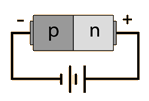
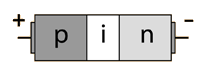
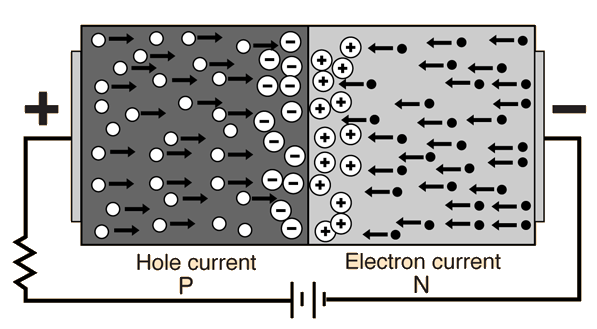
Forward Biased P-N Junction

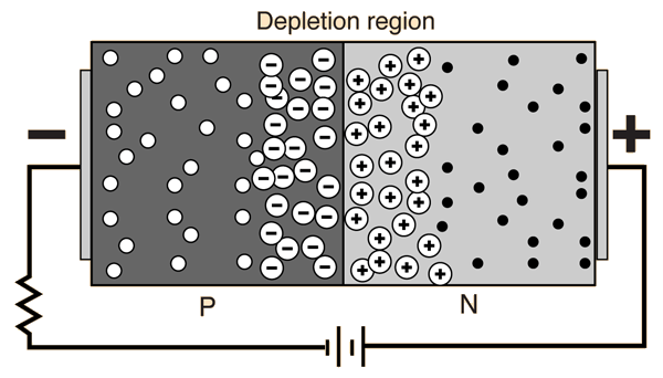
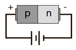
Forward biasing the p-n junction drives holes to the junction from the p-type material and electrons to the junction from the n-type material. At the junction the electrons and holes combine so that a continuous current can be maintained.
Show energy bands.Compare to reverse bias.
Index

Semiconductor concepts

Semiconductors for electronics
 
HyperPhysics***** Condensed Matter R Nave
Go Back


Reverse Biased P-N Junction

The application of a reverse voltage to the p-n junction will cause a transient current to flow as both electrons and holes are pulled away from the junction. When the potential formed by the widened depletion layer equals the applied voltage, the current will cease except for the small thermal current.
Show energy bands.Compare to forward bias.
Index

Semiconductor concepts

Semiconductors for electronics
 
HyperPhysics***** Condensed Matter R Nave
Go Back


The P-N Junction Diode

The nature of the p-n junction is that it will conduct current in the forward direction but not in the reverse direction. It is therefore a basic tool for rectification in the building of DC power supplies.
Diode varietiesPIN diode Step-recovery diode Diode applications
Index

Semiconductor concepts

Semiconductors for electronics
 
HyperPhysics***** Condensed Matter R Nave
Go Back


The PIN Diode

The PIN diode has heavily doped p-type and n-type regions separated by an intrinsic region. When reverse biased, it acts like an almost constant capacitance and when forward biased it behaves as a variable resistor.

The forward resistance of the intrinsic region decreases with increasing current. Since its forward resistance can be changed by varying the bias, it can be used as a modulating device for AC signals. It is used in microwave switching applications.
Index

Semiconductor concepts

Semiconductors for electronics
 
HyperPhysics***** Condensed Matter R Nave
Go Back


Step-Recovery Diode

In the step-recovery diode the doping level is gradually decreased as the junction is approached. This reduces the switching time since the smaller amount of stored charge near the junction can be released more rapidly when changing from forward to reverse bias.

The forward current can also be established more rapidly than in the ordinary junction diode. This diode is used in fast switching applications.
Index

Semiconductor concepts

Semiconductors for electronics
 
HyperPhysics***** Condensed Matter R Nave
Go Back